


 Your new post is loading...

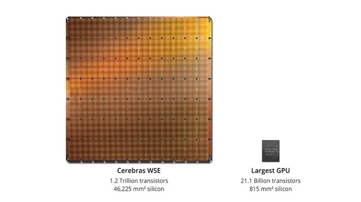

What is wafer-scale integration? A wafer is a circle, today about 12 inches in diameter. A chip is typically a square no more than an inch on a side — much smaller than a wafer. Many copies of the same chip are printed onto the wafer. They are arranged into a grid with spaces called scribe lines between them. The wafer is then cut along those scribe lines into individual chips. The chips are tested, and after any defective ones are discarded, the rest can be packaged and sold. Wafer-scale integration is the idea that you make a single chip out of the whole wafer. You skip the step above concerning cutting the wafer up — with one chip there is nothing to cut.


WHY IT MATTERS: this new technology enables new possibilities for machine learning applications such as autonomous driving. Tesla has recently announced that every car since 2019 contains a special chip that enables autonomous driving. This wafer-scale technology takes the same concept to another level.
http://fmcs.digital/blog/all-the-data-self-driving-cars-take-in-from-cameras-looks-like-this-and-the-webviz-tool-to-visualize-it-is-now-open-source-will-this-lead-to-faster-adoption-of-self-driving-car-technology/